Showing posts with label pcb. Show all posts

Tuesday, November 20, 2012

Etching heater

Etching with Ferric Chloride is a messy business. So the quicker you can get it over with the better - and for a few reasons. One way to decrease the time taken to etch is agitation: basically stir the mixture or dunk the board in and out of the etchant.

The problem with this, of course, is more opportunity for spillage. And with ferric chloride being such a nasty staining solution, you don't want it splashing around the place.

Another way to speed up etching is using heat. Ferric Chloride works best at about 50 degrees. But sitting the solution in a bath of hot water only increases it's temperature by a few degrees at best. So we tried one of these things - it's called an etching heater, but really it's just a fancy aquarium heater!


It's like a super-duper tropical aquarium heater in a sealed glass case- complete with temperature control on the top, so you can set the thermostat to anywhere between 40 and 60 degrees: perfect for ferric chloride etching! Just search ebay for "etching heater". This one cost less than �15 including delivery to the UK and took about 8 days to arrive.

We put about a litre of ferric chloride solution (made up quite strong, with a full 500g packet of crystal dissolved into about 1L of warm water) into a sweetie jar. This should allow us to etch rather larger boards if we need to. Just stand the heater in the solution, switch on and back away. After about five minutes, the entire thing is up to perfect etching temperature.

(heating the solution is easy - plop in the heater and switch on!)

A relatively small board can now be etched in about two-to-three minutes, rather than the 15-20 minutes it has been taking recently, when etching "cold" (as the winter nights draw in, it does get colder in the nerd cupboard, so ambient temperature is about 16-20 degrees).


The great thing about etching quickly is that because the board is in the solution for a lot less time, the chance of under-cutting is much less (under-cutting is where the etchant eats away at the copper under the toner-transfer mask because the board is left for too long in the solution). By etching hot and quickly, we get really sharp, clear etching, even with thin traces. 


In the photo above, we've managed to get traces down to 0.2mm and they've etched perfectly. When etching "cold" we would rarely go below 0.38mm trace size to avoid over-etching the tiny thin traces.


Here's the board cleaned up, with a micro sd card connector soldered in place, ready for populating. In short, 

Sunday, September 23, 2012

BuildBrighton PCB making workshop

Yesterday (Saturday) was BuildBrighton's PCB making workshop, as part of the Brighton Digital Festival.
From a worryingly quiet start, we ended up with six people taking part in yet another successful practical workshop - 100% success rate!

Over six hours, we introduced the attendees to schematic drawing using ExpressPCB (it's much simpler and easier to get going with than Eagle for anyone new to electronics/PCB layout) and their PCB layout software. A few people had brought along projects that they were working on and we helped them create PCBs for their own creations, while everyone else set about recreating the famous BuildBrighton Drawdio  kit.

(all the tools needed for making your own PCBs, including ExpressPCB software, press-n-peel blue paper, ferric chloride, a sanding block and a heavy duty laminator!)i

Sadly, the workshop was such as success and everyone was having such a lovely time that we forgot to take any more photos! But, for reference, for anyone who attended and would like to know more:

The first step was to create/draw your schematic (the bit with the little squiggles and symbols for electronic components). The most important thing to remember here is to give every component on the drawing a unique Part ID (the name can be anything, it's that part id that's referenced in the PCB layout software)

Then we drew our actual PCB layout using ExpressPCB.
File -> Link schematic to import the list of part IDs used in our circuit. A lot of people found it easier to drop symbols for all components used onto the screen before starting the layout process (menu Component -> Component Manager). Make sure that all components are drawn on the top (red) layer!
The most important thing to remember here is no crossing the lines!
In a few instances, some people ended a trace with a round pad, allowed another trace to pass "through" and started the trace again the other side, with another pad


Where a trace is continued after allowing another to "pass through" we tend to draw a connecting line on the silkscreen (yellow) layer, to act as a reminder when assembling the final board.

Once the PCB layout was complete, it was time to get on with the toner transfer.
For our workshop, we used Press-n-Peel (blue)


Toner transfer paper tends to be quite expensive, so rather than just print straight onto the blue sheet, we printed our PCB layout onto plain paper first (using a laser printer - inkjet just won't work for this!). Then cut out a piece of p-n-p blue just a bit larger, stuck it over the printed image with regular tape (shiny side down, powdery side up) and re-printed the image. This gets the PCB image onto the smallest sized bit of press-n-peel, meaning you've got plenty more left for another go!

With the image on the press-n-peel, we cleaned up some copper clad board (available from various online suppliers - eBay sometimes is a cheap source) using a fine-grit sanding block.
Sanding the board not only cleans it up (it needs to be bright and shiny and all traces of oxidation removed) it also provides a slight "key" for the toner image to stick to when transferred.

Tape the image (face down) onto the shiny copper board using paper-based masking tape, preferably cut to fit into a corner of your copper board (so it takes less cutting later). It's important not to use sellotape or similar plastic backed tape, as this will melt during the transfer process.

We used a heavy-duty laminator, but you could also use a regular household iron.
After three passes through the laminator, the image is transferred onto the copper board. Douse in cold water (carry the board by its edges, it gets very hot!) and carefully peel off the backing.


When done correctly, there should be no black traces left on the backing sheet. Check all traces carefully on the copper board. Where necessary, touch up any missing detail with a fine-tipped permanent (black) pen.
When happy with the transferred image, it's time to actually do some etching!

Ferric Chloride (FeCl) is messy stuff. Make sure you're wearing your old clothes and get ready to clean up any spillage immediately (it stains!). We made up a small batch using hot water and about a quarter of a pack of crystals. Etching in warm solution is quicker than in cold, although the end result(s) are the same.

The Ferric Chloride solution should be a dark brown in colour. If it's pale yellow, you need to add more crystals. If it's an orange-y colour, it will probably work but will take a long time. If you're re-using old solution (that's already had a few boards etched) and it's a dark green-y colour, it's getting a bit old and you should consider refreshing it. A dark brown (which is a golden yellow colour at the edges) is the perfect strength mix.

Submerge the board and either tip the container slightly to wash the mixture over the board (large boards in a small, shallow contianer) or dip the boards in and out of the mixture (smaller boards, suspended in a tall container on bits of wire). It will take 10-15 minutes for the board to etch completely.

The copper board etches in a couple of stages and if you keep checking it regularly, you'll see:
Firstly, the board goes a very vibrant pink.
Then the edges of the board (where the copper is exposed) start to look a little bit green.
Finally, the edges of the board turn a beige colour (the natural colour of the board the copper was stuck to) and the etching continues, usually from the edges, towards the centre of the board)

When no trace of copper remains (double-check for little bits of pink between the black traces on the board) your PCB is fully etched. Congratulations!

Some people prefer to drill then clean their boards - we did it the other way around.
You can use nail-varnish remover or similar acetone-based cleaner, or simply scrub with a fine-grit sanding block until all traces of the black toner are removed and you're left with a shiny new PCB.


During our workshop, everyone successfully made their PCB, etched and drilled to a finished standard! A few brave souls even populated their boards with the Drawdio components provided - and they worked!!

All  in all, another successful BuildBrighton workshop and a great day making stuff!


Friday, August 31, 2012

CNC drilling machine - testing everything

This is one of the most exciting blog posts for a while. After working on the CNC drilling machine as part of the BuildBrighton �50 CNC challenge for a few weeks, we're actually at the point of putting software, hardware, nc drill parsing and motor controller all together and actually trying to cut a PCB.

Actually, we don't have the drill part running yet - but this test shows actual movement, and we've used a laser dot in place of a drill head. But it shows a (sort-of) working CNC machine....


Instead of jumping in at the deep end and trying to draw a complex PCB (the printed pattern on the paper) we started off with a simple square. But as you can see from the video, we deliberately drew (and mounted) the square on an angle, to simulate mounting a PCB on the cutting bed on a wonky angle.

The software takes care of the rotation and follows the dots.
The first few seconds of the video show the machine being calibrated - the software prompts you to place the cutting head over a hole, record this location, then move the head to a second hole. This is what you see as the head travels diagonally across the board at the start (and the slight delay in the finer movement is us changing some parameters on the PC to reduce the jog step size).

The software then works out the cutting path (in this case, a simple down-across-up type pattern) and sets the motors spinning!

It's interesting to note that the cutting head doesn't necessarily follow the "lines" between the dots (if the dots were on the corners of a square for example), since it is a point-to-point machine, rather than a line follower. We'll try to demonstrate this more clearly in a later post.
But for now, sit back and enjoy our first CNC test.

It's not bad. It's not perfect - we need to take out any backlash in the gears (the motors themselves have quite a bit of "slop" on the spindle because of the internal gearing) to get greater accuracy but as an initial test - and particularly the handling of skewed boards - we're quite pleased with progress so far!

Next time we hope to actually cut (or maybe just draw felt-pen dots on) something.....

Tuesday, December 13, 2011

Blood Bowl board game slave board

Our intelligent Blood Bowl game board consists of two PIC micros which talk to each other via serial (during testing we're using 9600 baud but will crank this up for the final version). The slave board is simply a 40-pin 16F877A with pull-down resistors on all the digital i/o pins.


To allow for maximum flexibility, we're designing this slave board to accept as wide a range of PIC microcontrollers as possible, including some of the 18F series chips (if you have some hanging around from other projects, why not use them instead of buying in new?) Allowing for the power, ground, TX and RX pins (which are in the same place in the 40-pin 16F and 18F chips), as well as the useless Vusb pin on the 18F (useless in this case since we can't use UART and USB together) and the handshaking line we've got a maximum of 30 input pins (we could use the RX pin for handshaking, but for now we'll keep that clear in case we can come up with a use for it in future). In the diagram above, all available i/o pins have been taken out to a set of SMT (1206 sized) resistor pads, and all the resistors are tied to ground (making them pull-down resistors on each input).

30 inputs is an awkward number to work with since each board module is 4 squares in size the maximum number of inputs we can use is 28 (4*7=28). So we've got two free input pins on the slave board should the need arise, as we develop the concept further.


Slave Board

Saturday, December 3, 2011

Intelligent board game (Blood Bowl) development

Here are some photos of the latest board game development;
although we're working on a Blood Bowl clone, the same technology could - in theory - be used for a large number of games, with different board sizes. To date, we've settled on a 4-square module and will make our board game(s) up from this/these.

These photos are from our 4x2 boards (earlier design) but the principles work the same for both.
On the sides of each playing square (N,S,E and W) we drilled a 1mm hole and soldered some pcb studs


The studs are slightly raised on the playing surface of the game board. This isn't as nasty as it sounds - for our Blood Bowl game, it means we can add some "flocking" or similar covering but still get the playing pieces to make a good contact with the pins.

stupid cheap HP camera - even in "macro mode" it doesn't quite know what to focus on!

The plan is to weight our playing piece bases with a small copper disk (something like a 2 pence piece would be ideal, only we don't want to get thrown in prison for "defacing a coin of the realm" or whatever the punishment is these days!). Placing these on the playing side of the board bridges the two connections between the "rows" output pin on the master controller and the "columns" input pin on the slave - so when the slave is asked "which inputs are high/low" this can be used to work out which squares have playing pieces on them.

once again, a nice focussing job by our little HP camera

The tracking of which playing piece is on which square will be done by the master IC. For these early prototypes, we're more concerned about proving the concept of tracking which piece is being lifted/replaced to/from the board.

Thursday, December 1, 2011

Creating the playing squares for an intelligent board game board

While toner-transferring and etching our game board "modules" something became obvious - though it's not something we'd thought of when designing our PCBs. The photo below shows our game board etched onto a piece of eurocard sized (160mm x 100mm) copper-clad board


While trimming to size, we realised that the bit cut off the bottom was almost exactly the right size for a single row of 4 playing squares (the printed module above shows a 2x4 grid of playing squares). It then occurred to us that there's no real reason why we couldn't create modules that were 1x4 instead of 2x4.

After all, the top row still has to be connected to the bottom row using a wire jumper/via even when they are drawn/etched on the same piece of board. So here's the new PCB layout for four playing squares at a time:
Since the spacing of the playing squares is 30mm (standard Blood Bowl size) the PCB is also 30mm high (with the playing squares pretty much in the middle of each "strip" of 1x4 squares).
If you want smaller playing squares, simply resize the whole PCB. The overall size will shrink to match the size of each playing square so they should still be able to be cut to size and placed side-by-side, without affecting the spacing between playing squares.

4x1 Board Piece

As you can see, they line up perfectly for connecting horizontally once etched and cut to size:


A little bit of multi-core wire or maybe even some gloopy solder should connect the two boards, edge-to-edge.

Wednesday, November 30, 2011

Electronic board game - Blood Bowl clone

Some interesting developments over the last few evenings as we've put together all kinds of ideas for an intelligent board for a board game (like, our old favourite Blood Bowl).
Our original proposal - based on freeing up as many pins as possible from two 40-pin PIC microcontrollers - was to allow for up to 600 squares, or a grid of 20x30

To allow for as much flexibility as possible, while at the same time making it relatively easy to understand, we've decided on a modular approach. Our board game will actually be made up of a grid of 4x2 "blocks" which can then be wired together in any arrangement. It means we've lost the flexibility of really wacky board layouts (although using the same technology it should be possible to create one-off boards with pretty much any layout as required) but does mean that we can simplify making boards of different dimensions.
(it also means that anyone who buys their copper boards in eurocard 100mmx160mm size can still make a board game, using a "patchwork" of smaller boards)


4x2 Board Piece

Each playing square in this board is marked out by a "cross" shape on the board. Small through-hole studs are soldered to this underside, so that on the playing side of the board, a small contact point is visible on the playing surface. Each playing piece has a conductive base (a copper coin glued to the bottom would suffice!) and when placed over the four points of a cross, makes a connection between the top and right contacts and the bottom/left contacts.

Using the above layout, we can place these pieces side-by-side and join the edges, while connecting each group of top/right contacts together using short pieces of (insulated) wire


Using this approach, we've designed our Blood Bowl board.
It's not quite 30 x 20, but we found that vertically connecting 7 "rows" of 4 contacts means for each row we can read back up to 28 lines of "column" data. By placing four of these smaller boards side-by-side, our board size is 28 x 16 playing squares. Not a bad compromise and certainly a sizeable playing area for a lot of different board games.

So what does it look like? In short, a nightmare!


As you can see, each smaller board is connected to the board horizontally next to it (the traces were deliberately lined up to make this bit quite easy). Every 7 vertical rows of contacts are connected via wire traces (shown in this diagram by different coloured bars) and each group of these 7x4 = 28 contacts is then connected to the slave microcontroller via a short wire (the connection points for these wires are circled in a matching colour).

There are 16 wire connect points - these go to the master PIC. The 28 traces from the bottom/left sets of contact points are connected to the slave. By flashing one of the 16 wires at a time, and reading the input values on the 28 inputs, we should be able to work out which set(s) of contacts are being bridged by a playing piece on the board.

That's the theory anyway.......

Tuesday, September 6, 2011

CNC pick-and-place machine needed!

After spending hours and hours last night assembling and soldering just a couple of PCBs, the need for some sort of automation is growing - especially if we're going to realise the dream of actually making and selling a few miniature instruments.

So we're back to investigating a miniature CNC-type pick-and-place machine.
We've already got some stepper motors working and pulled apart a few printers and scanners, and have had no luck in finding exactly the types of steppers, belts and pulleys we were hoping to use.

Which has lead us down a slightly different path - instead of determining which types of stepper motors and belt-drive system we're going to use up-front, we're going to build a system which anyone else can build too - but using parts that can easily be scavenged from old computer hardware.

We dismantled an old Lexmark Z73 and found some useful looking stuff - stepper motors, carriage rods, belts and so on. None of these match our original cnc requirements (1.8deg steppers, 20-tooth pulley, 5mm pitch belts) but we've decided to change our approach, and build a machine using the parts we can get hold of. We'll write some software to drive our custom-made stepper board, so that you can simply enter a few parameters and let the computer do all the tricky calculations.

This sounds like we're heading towards Mach3/traditional CNC type ground - the original plan was to just build something that would work "out-of-the-box" without lots of difficult setting up and parameter fiddling. But then again, buying all new hardware is going to get quite costly for us, or anyone else wanting to make a similar machine, whereas re-using and recycling old computer hardware is a much more eco-friendly way to go about making stuff in general.

Here's our starting point - a stepper motor and a timing belt.


The stepper motor is a Mitsumi M42SP-6NK.
A quick look on Google returns the datasheet, telling us that it's a 7.5 degree motor, runs at 12V and has a peak current of 400mA. We marked one of the teeth on the cog, then counted them clockwise, and discovered that this motor is fitted with a 15-tooth pulley


The timing belt didn't reveal much - the serial number OPM 300766 returned nothing of interest, so we had to do a bit of investigating....


To find out the pitch of the belt, we need to measure from the centre of one tooth to the centre of another. This belt has tiny teeth, so we marked out 20 teeth using some masking tape and measured across the tops of the teeth with a steel rule (marked in 0.5mm spacing). Despite the photo's appearance, we made it 24mm across 20 teeth, making the belt pitch 1.2mm


This may or may not be correct. The belt may even use imperial measurement (e.g. 1.2mm = 0.0472 inches - it may be a 0.05" pitch belt and we've just not measured it properly!) All this can hopefully be corrected in software once we've actually got the machine built, entered a few parameters and calibrated everything fully!


Monday, August 15, 2011

PCBCart order is in

We've found making consistently good double-sided PCBs quite difficult of late, especially when we're working with tiny 0.20mm traces (normally we don't go lower than 0.5mm to ensure a good trace even if the etching goes a bit awry).


Having designed the PCBs for both guitar body and neck, we spent some time looking at different providers and suppliers. There are plenty of people on eBay offering PCB manufacture and we've already been in touch with quick-teck.co.uk.


Matt from BuildBrighton suggested PCBCart and in the time it's taken other PCB manufacturers to respond to an initial request for information, these guys have built gerber files from a simple design, debugged it, confirmed and organised all the silk-screening and solder-masking and submitted the plans for manufacture.


Their response times are amazing.

I was given the task of investigating PCBCart. I posted my order to them at about midnight and went to bed. The next morning there was an email from PCBCart asking to confirm a few things - after I emailed, I got a reply within minutes (not hours or days like other fab-houses) and in less than 30 minutes and a flurry of emails, the boards were ready for production!


I was really impressed with their service and how quickly and keen they were to get everything sorted out. After filling the online quote/order form out (they even accept PayPal) and paying a rather reasonable �140 for 200 pieces, our boards are in production and we hope to have them in about 12 days. If the quality of the manufacture matches their customer support, we should have some fantastic PCBs in less than two weeks - it's taken longer than that for some of the other manufacturers to respond to our initial query.


Hopefully that will be the last piece of the miniature guitar puzzle in place and we can start assembling them for real!


Sunday, August 7, 2011

Guitar PCB with DipTrace

Using DIPTrace we've got an SMT version of our guitar PCB already drawn out, etched and the components laid out ready for soldering


We made the pads on the crystal far too large for the SMT crystals we're using. But other than that, the extra sized pads look to be just right for hand-soldering


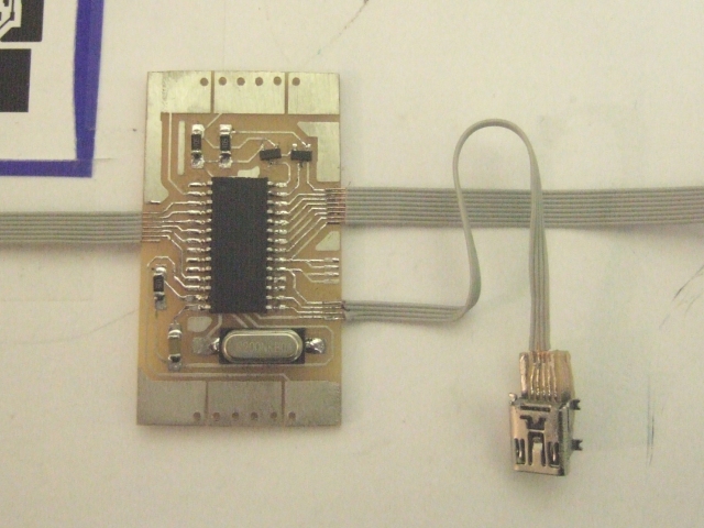
And about half an hour later (including time taken to tin plate the entire board) here is the same board, all soldered up


The miniature USB socket was a surface mount version, so had to be soldered onto a tiny breakout board to enable us to connect to the 0.025" pitch multi-core cable.


All that's left to do now is program the PIC and check everything works as it should. For the guitar neck, we'll need another (double-sided) PCB but for testing, we can touch the ends of the exposed multi-core wire to simulate how it will behave when wired up to the fretboard PCB.

Saturday, August 6, 2011

DIPTrace to replace ExpressPCB?

To date, our preferred PCB layout software of choice has been ExpressPCB.
It's a brilliant bit of kit, easy to use, simple to build your own components, and best of all - FREE! For through-hole work it's really easy to use - draw everything you want on the top (red) layer and print straight onto your press-n-peel. Admittedly getting a usable output for SMT is a bit fiddly at first (install CutePDF then print your boards to a PDF file, load into Inkscape, mirror/flip horizontall and THEN print) but it's nothing that takes more than a minute or two to sort out.

Since we discovered Quick-Teck we've had to give serious consideration to gerber files. Until now, we've never bothered with them - and as a result had no need to learn how to use the, frankly, clunky Eagle interface. But after getting a quote from quick-teck.co.uk for PCB manufacture, and a second one for sourcing the components and assembling the board, we're seriously considering getting our boards supplied ready-assembled.
The problem with this approach is that while PDF schematics and layouts are fine for making your own boards via toner-transfer, and for using to get a quote for a job, they're not really acceptable for making the circuit boards from. Most PCB manufacturers prefer gerber files and Quick-Teck are no different. Which means we're probably going to have to get friendly with Eagle.....

... or does it?
In our recent trials of different PCB software, we gave RS Component's DesignSpark (PCB design and layout software) a go. Like many companies keen to get in on the maker scene (think Farnell/element14, AutoDesk etc) RS are giving away free software to lower the barriers to get the community involved. The problem we found with DesignSpark is that it was too much like Eagle - complicated and clunky. One thing we did like, however, was that when drawing a schematic, clicking between two sets of pins drew a nice connecting line, with 90 degree bends automatically drawn in the appropriate places: drawing schematics like this is quite nice.

With an inherent dislike of Eagle, and having dismissed DesignSpark, we went looking for alternative software and stumbled upon DipTrace.

DipTrace is a really nice, simple, intuitive PCB design and layout application. It does the nice "semi-auto-complete" drawing on schematics- and then extends this to the PCB layout application too. It has full component auto-place AND trace auto-routing (we haven't used either of these for our projects, but it's nice to know it's there) AND includes helpful auto-drawing when placing traces by hand.

In short, we think DipTrace is an excellent bit of kit.
It's as simple to understand as ExpressPCB, making your own components and layout patterns is a doddle and it has all the fancy export options you'd expect to find (including dxf and gerber). Hobby users haven't been forgotten either - from the print preview screen you can mirror the output (for toner transfer/press-n-peel users) and it even has a "outline the traces for CNC output" option for anyone who wants to rout the traces out from copper clad board on a CNC routing machine.

It took us just a few hours of playing about tonight to not only create a library of our most commonly used components (amended to include big fat pads for easy soldering) but also to draw an intermediate-level schematic and layout the PCB for it. In less than three hours we had a board printed and ready for etching. After three hours with Eagle we were still trying to work out how to move more than two components without screwing up the entire design!

Look out for future posts detailing how to use DipTrace.
We'll be using it a lot in future and hope to convert a lot of our earlier projects using it - starting with our current miniature guitar project.

With a free non-commercial licence (2-sided board, up to 500 pins) you'd have to be a pretty hardcore user to need to upgrade - by which time you shouldn't mind paying the relatively modest licence fee for the full package!

Friday, August 5, 2011

Guitar PCB boards - SMT rules!

After initial reluctance, we're getting to quite like the idea of using SMT circuit boards for our miniature instruments. True, soldering them can be a bit fiddly - especially with a massive tipped soldering iron - but that can easily be fixed by using a smaller nib.

Even so, with a large tip we've managed to solder some pretty teeny little components.

Another benefit of using SMT is that everything is done on just one side of the board. With through-hole, all the components are on the "top" but on the underside are lots of little spiky bits where the component legs have been soldered to the copper board and trimmed. SMT gives us a nice flat surface on the underside to work with. A bit of double-sided tape on the unused side -


- and the board can be stuck to the acrylic "lid" of the guitar -


- and a nice flush finish, so threading the strings through from the top-side should be a doddle


Compare that to the original design, where getting the strings to line up with the holes, holding everything together AND soldering everything in place was a bit of a nightmare!


In fact, as part of our recent board edits, somehow we've managed to reduce the board length a little bit so the holes on the board don't line up with the holes on the acrylic. They're only a few millimetres out, but it will make quite a difference if we fix the board flush to the underside of the plastic. Then again, it's not a massive problem to sort that out.
There's a good chance we'll be making PCBs for a while yet, until we settle on a final design!

Thursday, August 4, 2011

Laser cut solder paste stencils

Well, we've decided to give SMT a try again, for making our guitar PCBs. So the first thing to do is make an SMT version of our earlier (working) guitar board:

We tweaked it a bit - making some pads bigger and spacing a few out more. We also had problems with the first version of the board, connecting the guitar strings to the two rows of six pads at the top and bottom of the board. If we didn't take care soldering, the round pads would lift quite easily, so we've changed them slightly for this board.


This board was designed in ExpressPCB, printed to PDF using CutePDF then opened in Inkscape to flip it horizontally (mirrored) so the final transfer was the right way around - when you're working with through-hole components, you actually want the PCB to be mirrored on the underside so print it as you see it works fine. For SMT work, the image needs to be mirrored so that when it's transferred onto the copper board, it ends up the right-way around.

With our fancy new laser cutter (how longer before it stops being fancy and new, and just becomes "our laser cutter" I wonder?) we cut a stencil design into an acetate sheet. We won't do it again - acetate stinks! And it burns and browns and covers everything in a sticky goo. But here's the solder paste stencil we made anyway:


Maybe the stencil holes aren't fine enough, or maybe we didn't use it correctly, but after applying solder paste through the stencil, we just ended up with big blobs of paste on the board. Manually applying the paste with a small paintbrush may not give a better result, but is about ten times quicker to do!


So we cleaned the board off and applied the paste again using our tried-and-tested method with a small brush


Even with quite a large tip on our soldering iron we got quite satisfactory results. Simply touch the tip onto the pad to start the paste flowing. Any paste in the gaps between traces simply burns off (or flows onto a tinned pin). To be sure of a good contact, we touched the tip of the iron onto the pin to be soldered to make sure the solder doesn't just flow under it.

You may see solder on the bits of board between traces. On a professionally manufactured board, these bits would be covered with solder resist. This is where we just applied solder paste all over the pins then heated it to remove the bridges between traces. Obviously, where the solder paste settled on these "in-between bits" it's resulted in excess solder on the face of the board. We *could* have etched all this excess away and not bothered putting a "solid plane" between traces - but then the Ferric Chloride would take an age to etch the board fully.

Here's the finished board, with multi-core cables attached on one side.
It's not a complete working board, but we've proved that we can solder SMT components just as quickly (we're not going to say as easily!) as their through-hole counter-parts.


On a professionally manufactured board, with solder resist and only the pads exposed, soldering would be even easier - but we found hand-soldering SMT components onto a home-made board relatively straight forward (and pretty quick to do!)

In the example above, we tried two different types of wire - what we're calling "half-pitch" (0.025") IDE cable and "regular" 0.5" IDE cable. We thought that the bigger cable would be easier to solder to the board but thought we'd try the two side-by-side to compare them. Although the regular cable is easier to solder (the traces can be bigger and slightly wider spaced) it's also more likely to fail when working on a large number of boards - because each core is multi-stranded, you have to take great care when soldering as the strands can fan out and easily create bridging with the other contacts. The smaller cable is a bit more fiddly to work with, but because each core is solid, once it's in place, there should be no worries about bridging with other wires.

We've yet to settle on a final design but whichever we choose, will probably be a compromise between easy of soldering and likelihood of failure - we want something that's easy to put together, but if we're likely to get a high failure rate, we'd be better off spending a bit more time on something a bit more fiddly, but be confident that it'll work once it's done!

Wednesday, August 3, 2011

We're through with drilling

See what we did there? Through with drilling? Because we're only drilling the PCB to allow us to use through-hole components. Clever huh?

Honestly, when you have to explain a pun it makes it really lame.
Anyway, in the search for an easy-to-make circuit board that can be soldered quickly and repeated easily, and since we're trying out old ideas once more, we've decided to give SMT a go again.

This time, things will be different.
For a start, we can tin-plate the PCB before soldering. We already know that this makes soldering easy, to the point where we're able to solder tiny 0.025" pitch cable to an edge connector on the board.

In fact, using the tin-and-solder-paste method, we attached the multi-core cable much quicker than we ever could if we were using the older method of splitting the cable and soldering each strand through a series of 0.1" pitch holes.

With all this in mind, we figured we give SMT a go again.
We've already got a selection of SMT components in our tool box - mostly 1206 sized resistors and capacitors, and some SOT23 darlington transistors. The SMT crystals from Farnell are the same size as the through-hole versions, only with tabs instead of legs.

The only thing we haven't got is an SMT version of the PIC 18F2455 microcontrollers we've been using. But we thought we'd print out an SMT version of the body PCB and see if the components we had were suitable.


In this example, the ribbon cable(s) to connect the main board to the neck is our tiny 0.025" pitch IDE ribbon cable. We already know we can solder this to the edge connectors, quickly and relatively easily.


Another benefit of using SMT components is the non-copper side of the PCB will be completely empty and we'll have no nasty spiky bits of wire poking through the bottom. So we'll have a nice, low-profile board, a flush reverse side that we can stick straight onto the underside of the guitar top, and no nasty messy tangle of wires like we had on our first attempt.

Of course we'll still need to keep the two rows of six holes along the top and bottom edges of the PCB, since the strummer strings still need to pass through the board from the top of the guitar. But this new layout now requires only 12 holes instead of the seventy or so in the original design.

Inspired by Crazy Dave in this eevblog video (below) we reckon soldering a whole load of SMT components might actually turn out quicker than using their larger, chunkier, through-hole versions.


In fact, if the prototype board works we might just head over to http://www.quick-teck.co.uk and get some double-sided boards professionally made up. Check the spelling to get your browser over there!

All-in-one guitar PCB

Since we're re-visiting old ideas (creating a neck PCB with traces rather than soldering wires to pins) we thought we'd try out another old idea - creating a single PCB for both the neck and body as one piece


It means we'll have to re-think the enclosure - at the minute it's been designed around how an actual guitar looks, with the neck raised slightly in relation to the body. If we're using a single-piece PCB, when the plastic front of the guitar is put into place, the fretboard (the reverse of the PCB) is about 3mm lower than the body. Then again, this would provide us with an opportunity to use a real wood laminate on the guitar neck for a more realistic fingerboard.

We also need to consider how the through-hole components affect the position of the guitar neck in relation to the body...

Guitar PCB take two

Not only are we trying to make a working miniature guitar, we're also trying to find the best (and easiest) way to make a number of them, in a way which is consistent and repeatable. So far we've managed to make a working instrument, but it was really fiddly to make, and for anyone else to try to follow the same steps, it'd be pretty hit-and-miss as to how successful the end result would be (we're not mentioning that our guitar didn't actually fit into it's enclosure!)

So we're trying out an old idea again - making the neck PCB from fine (0.2mm) traces and connecting via a ribbon cable at one end. Here's the design toner transferred onto some copper clad board:


The board was cut to size to make sure it fit along the guitar neck. In fact, we can be quite loose with measurements and tolerances- at this stage, once we have a working PCB design, we can always amend the acrylic shape(s) to fit the PCB if necessary


Then the board was etched and the edges sanded and finished off nicely


Some half-pitch IDE cable was attached (I think this is 0.025" pitch cable. Whatever it is, it's about half the pitch again of "regular" hard drive IDE cable). This was acheived by tin-plating the end of the PCB first (it was too big to fit inside the glass jar we keep our tinning solution in)


Using our new tin-plating and solder-paste technique, the ribbon cable was actually quite easy to attach, even with a big fat pointed tip on the soldering iron. Maybe the fact the IDE cable was made up of single solid cores helped.

The larger "blob" of solder came off the tip of the soldering iron when we started the second piece of multicore cable. It's actually a tiny little bit of solder, but looks enormous on this photo!

The cable ends were checked for continuity and the new-style PCB put into place to make sure the ribbon cable wasn't too wide for the opening


Compare the amount of loose wire with the new board and the old one. With the new board, we could simply loop the multi-core cable under the entire main board PCB and attach to an edge connector.


We considered an alternative - creating a single, solid piece PCB for both the body and neck in one go. This has the advantage of being easier to assemble (although etching requires a shallow bath rather than our preferred "dunk-in-a-coffee-jar-of-gunk" approach) but the downside is that the guitar neck would appear lower than the guitar body (once the acrylic top layer is in place).


We were keen to keep the guitar fingerboard higher than the guitar body so that it accurately reflected the construction of a real guitar


To date the only way we can see this working is to have the guitar neck as a separate board, attached to the main board via a ribbon cable. If we used a single piece PCB, we could make the acrylic of the guitar neck from 3mm instead of 5mm to reduce the height (reducing the position of the body part of the PCB) and introduce a layer on top of the neck PCB, making it appear raised higher than the body?