Showing posts with label diptrace. Show all posts

Wednesday, November 21, 2012

DipTrace for home etching, gerber export, 3d views and milling outlines

The more time we spend with DipTrace, the more we like it, here at Nerd Towers.
We first came across it while designing PCBs for our miniature guitars last year - changing over from ExpressPCB because we needed to generate gerber files to have some circuit boards manufactured online.

It's easy to use, has a massive library of components, but uses an approach similar to Eagle; when placing components in the schematic, you have to choose the "correct" component with the appropriate footprint while you're drawing the schematic. We much prefer the ExpressPCB method: draw a schematic then link it to the PCB designer - so long as the number of pads in the PCB layout software matches the number of pins in the schematic, you can use pretty much any component footprint to represent any component in the schematic.

As a result, we still turn to ExpressPCB whenever we need to "knock out" a few boards for home etching.
But since we've had to design some more boards for manufacture (for a recent alarm clocks project) we've returned back to DipTrace to generate more gerbers.

And we've found that DipTrace has some pretty cool features - even for the homebrew enthusiast. Firstly, you can create homebrew boards easily and - using the ExpressPCB method - print to a PDF file using CutePDF and flip in Inkscape, reading for printing onto some press-n-peel.


Of course, DipTrace can export to Gerber (so the file(s) can be emailed for manufacture by a professional PCB fabricators). But it also has a few other handy export options.

We've already discovered the brilliant 3D view:


The great thing about this 3d generator is that you can place components so that they "hang off" the board. Not many tools let you do this. In the example above, we've created our audio board but cut the dimensions down, so that the SD card holder is fixed at one end. There's no need to waste copper board under the rest of the sd card holder - not all PCB layout tools allow you to create a board outline smaller than the components on it!

As well as 3D, and creating toner-tranfer images, DipTrace supports exporting to DXF.
Why is this so impressive? Well, if you've a CNC router, you can get it to draw around the outside of each of your pads and traces:


Wow! Now that's cool. Anyone with any experience of using Mach3 or similar CNC software knows that it's relatively easy to get from a DXF drawing to some g-code which we can use to drive the CNC router and - rather than all that nasty etching with stinky chemicals - we could rout out the PCB board from a sheet of copper-clad board.

All these output options from the same PCB layout. DipTrace is looking like a really useful bit of kit. And perhaps something we should persevere with for a little while. After all, up to 500 pins, it's FREE as well.

Friday, November 16, 2012

DipTrace and the amazing 3D render

I recently had to get some PCBs made up for a little project, so had to leave my favoured ExpressPCB behind and use DipTrace again, in order to generate some gerber files for manufacturing (normally we'd just etch our own boards, but time is tight with this one, so they're on a three-day turnaround from a UK-based manufacturer).

I was looking for a gerber viewer when I came across Jason's post about a web-based 3d renderer: https://plus.google.com/u/0/105009608886388132613/posts/1oST39owVAZ

Now that looked exciting. I uploaded the gerber files generated from DipTrace and eagerly waiting for the image to appear..... nothing. Whether it was the gerber file, my lack of 3d graphics hardware in my little notebook or something else, I don't know. I do know that other people commented that they couldn't get it to work either. So no 3D renderings for us.....

Then I spotted this little icon on the toolbar:


So what would that do....?


Ta-da! A perfectly rendered (and populated) PCB. I'm not quite sure how to get the components to sit down in the board properly (seriously, who solders their components so they stand up like that?) but as a quick overview of how your final board could look (especially now we're moving away from through-hole and trying to use SMT wherever we can) it gives great results!

We might just give DIPTrace another go.
Familiarity and laziness have kept us using ExpressPCB. But these 3D renderings do add a fresh dimension to documenting projects (-no- pun intended) so maybe it's time to give it a whirl. The freeware version is quite restrictive with only 300 pins allowed. But for simple, little projects like this one, that's more than enough!

Sunday, August 7, 2011

Guitar PCB with DipTrace

Using DIPTrace we've got an SMT version of our guitar PCB already drawn out, etched and the components laid out ready for soldering


We made the pads on the crystal far too large for the SMT crystals we're using. But other than that, the extra sized pads look to be just right for hand-soldering


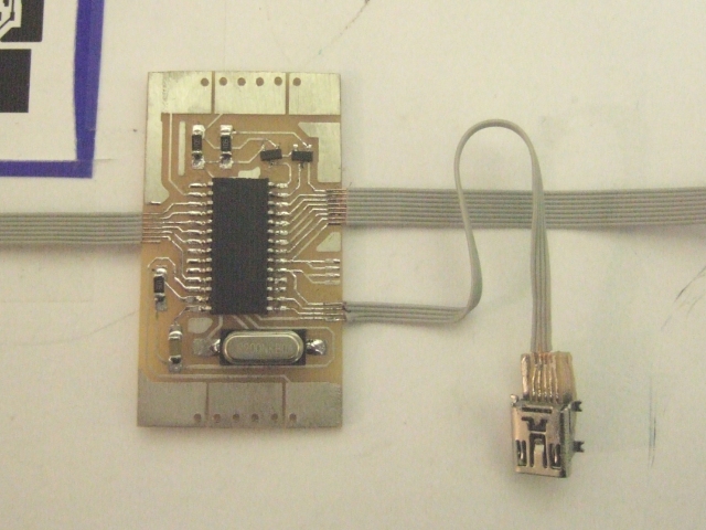
And about half an hour later (including time taken to tin plate the entire board) here is the same board, all soldered up


The miniature USB socket was a surface mount version, so had to be soldered onto a tiny breakout board to enable us to connect to the 0.025" pitch multi-core cable.


All that's left to do now is program the PIC and check everything works as it should. For the guitar neck, we'll need another (double-sided) PCB but for testing, we can touch the ends of the exposed multi-core wire to simulate how it will behave when wired up to the fretboard PCB.

Creating custom components with DIPTrace

Whenever we design and layout PCBs for homebrew manufacture, there always comes a time when we have to undo a great deal of work, and amend the footprints or patterns for the components on the PCB layout. This is because most PCB packages use "standard" pins and pad sizes, which - while fine for mechanised pick-and-place and SMT soldering machines - can be a nightmare to solder by hand. Whenever we've made a PCB we've always had to create a library of custom layouts - even when the PCB software includes libraries of common components from a variety of different manufacturers.

Because we're getting to like DipTrace very quickly and plan to use it for all our PCB work in the immediate future, the first thing we need to do is re-create our library of custom layouts.

Here's a quick overview of how to do this using DipTrace:

Start the DIPTrace pattern editor application. Create a new library (or open an existing custom library if you're adding to one you've already started) and from the [Pattern Menu] select [Add New To Library]

Fill in the name and RefDes values. RefDes is what is used every time a new instance of this component is added to your PCB. We've used IC so that when a PIC 18F2455 is added to our designs, it will automatically be labelled IC1, IC2 etc.


For this part, we're drawing a 28-pin SOIC chip (SMT version of the 18F2455) which consists of 2 rows of 14 pins. DipTrace includes an "add-row-of-pins" option. As you drag your mouse, it tells you how many pins it has put down


Select all the pins then right click on one of them to edit the properties


Changing the X and Y values affects only the first pin selected, but changing the height and width of the pin(s) affect all selected pins.


Depending on how your environment is set up, the pads may not be the correct type at this stage. We changed the pad type to rectangle, set the hole size to zero and the pad type from "through-hole" to "surface".


You should see a row of 14 pins- select them all and right click to copy


Paste a new row of pins and draw a rectangle between them (this will form the silkscreen layer later, showing where and how the IC chip should be placed on the board)


Check out the component datasheet to find out pin sizes and spacings.
In this example, we can see that our rows of pins need to be 7.5mm apart (the E1 value in this diagram)


Double-click each pin to amend it's height/width and X/Y values.
Note that DipTrace works from the centre of each pin as the origin. So if you have a pad that is 4mm wide, and you want a 7.5mm gap between pins, you need to consider the pad size when calculating the X/Y values.

For example, if you have the left hand pads at zero, the left hand edge of the pad starts at -2mm and the right-hand edge of the pad would be at 2mm. If you place the opposite pad at 7.5mm, the gap between the pads would be less than this. Because the left-hand pad overlaps by 2mm, and the right hand pad overlaps by the same amount, the gap between the two pads would be only 3.5mm (7.5mm less 2mm from the left-hand pad, less 2mm from the right-hand pad = 3.5mm)

So to get a gap of 7.5mm between the pads we actually need to start the second row of pads at (7.5 + 2 + 2) = 11.5mm

When you're happy with the pad placement save your pattern and start the DipTrace schematic software. Place the PIC18F2455 component into the schematic. You should notice that when a component is added to the schematic, a PCB layout pattern is also included. Double-click the component (or right-click to select properties) and click the "attach pattern" button to change the PCB pattern for this component


Select your custom library from the pop-up window and select the new pattern layout you've just created. Repeat for any and all components in the circuit.


And that's how easy it is to create your own custom PCB layout patterns for components and use larger-than-average pad sizes to help when it comes to soldering!

Saturday, August 6, 2011

DIPTrace to replace ExpressPCB?

To date, our preferred PCB layout software of choice has been ExpressPCB.
It's a brilliant bit of kit, easy to use, simple to build your own components, and best of all - FREE! For through-hole work it's really easy to use - draw everything you want on the top (red) layer and print straight onto your press-n-peel. Admittedly getting a usable output for SMT is a bit fiddly at first (install CutePDF then print your boards to a PDF file, load into Inkscape, mirror/flip horizontall and THEN print) but it's nothing that takes more than a minute or two to sort out.

Since we discovered Quick-Teck we've had to give serious consideration to gerber files. Until now, we've never bothered with them - and as a result had no need to learn how to use the, frankly, clunky Eagle interface. But after getting a quote from quick-teck.co.uk for PCB manufacture, and a second one for sourcing the components and assembling the board, we're seriously considering getting our boards supplied ready-assembled.
The problem with this approach is that while PDF schematics and layouts are fine for making your own boards via toner-transfer, and for using to get a quote for a job, they're not really acceptable for making the circuit boards from. Most PCB manufacturers prefer gerber files and Quick-Teck are no different. Which means we're probably going to have to get friendly with Eagle.....

... or does it?
In our recent trials of different PCB software, we gave RS Component's DesignSpark (PCB design and layout software) a go. Like many companies keen to get in on the maker scene (think Farnell/element14, AutoDesk etc) RS are giving away free software to lower the barriers to get the community involved. The problem we found with DesignSpark is that it was too much like Eagle - complicated and clunky. One thing we did like, however, was that when drawing a schematic, clicking between two sets of pins drew a nice connecting line, with 90 degree bends automatically drawn in the appropriate places: drawing schematics like this is quite nice.

With an inherent dislike of Eagle, and having dismissed DesignSpark, we went looking for alternative software and stumbled upon DipTrace.

DipTrace is a really nice, simple, intuitive PCB design and layout application. It does the nice "semi-auto-complete" drawing on schematics- and then extends this to the PCB layout application too. It has full component auto-place AND trace auto-routing (we haven't used either of these for our projects, but it's nice to know it's there) AND includes helpful auto-drawing when placing traces by hand.

In short, we think DipTrace is an excellent bit of kit.
It's as simple to understand as ExpressPCB, making your own components and layout patterns is a doddle and it has all the fancy export options you'd expect to find (including dxf and gerber). Hobby users haven't been forgotten either - from the print preview screen you can mirror the output (for toner transfer/press-n-peel users) and it even has a "outline the traces for CNC output" option for anyone who wants to rout the traces out from copper clad board on a CNC routing machine.

It took us just a few hours of playing about tonight to not only create a library of our most commonly used components (amended to include big fat pads for easy soldering) but also to draw an intermediate-level schematic and layout the PCB for it. In less than three hours we had a board printed and ready for etching. After three hours with Eagle we were still trying to work out how to move more than two components without screwing up the entire design!

Look out for future posts detailing how to use DipTrace.
We'll be using it a lot in future and hope to convert a lot of our earlier projects using it - starting with our current miniature guitar project.

With a free non-commercial licence (2-sided board, up to 500 pins) you'd have to be a pretty hardcore user to need to upgrade - by which time you shouldn't mind paying the relatively modest licence fee for the full package!