Today most robots are vacuuming homes or on the battle field. Instead this little robot is building stairs. Meet Kali, the little hard working stair building robot. This bot is part of Harvard's Termes Project, and they are working on creating a swarm building system with a lot of little robots that build something together.
The word "Termes" comes from termites and like termites these bots work together to building something. Termites work together in swarms to build mounds and these robots team up to build other things. These terms robots are autonomous, small, and simple, and they each have the capability of lifting and moving blocks to create things. Check out the video above to see them in there building action!
Tuesday, June 21, 2011

Getting Your Company On Facebook
Facebook has been a great resource for us to show the world our services at JC Gibbons Manufacturing. It can be a venue to show of pictures or videos of our products and services, but most importantly, it is a venue to keep in touch with our clients and potential clients on a daily basis. The site boasts any easy way to make a post and it has the ability for one-on-one chat which can be a great tool.
We think it will be a great tool for those that we do business with, so we wanted to make sure that this information is easily available. First off, visit the information page from Facebook about creating a page: create a fan page here.
Then you'll hit that green button in the top right corner to create a page, and you're off and running. It shows you how to create all the information for your business including adding a picture to your profile. It even shows you how to make contacts and how to use it to run ad campaigns similar to Google Adwords. It is just a great place to make connections.
We think it will be a great tool for those that we do business with, so we wanted to make sure that this information is easily available. First off, visit the information page from Facebook about creating a page: create a fan page here.
Then you'll hit that green button in the top right corner to create a page, and you're off and running. It shows you how to create all the information for your business including adding a picture to your profile. It even shows you how to make contacts and how to use it to run ad campaigns similar to Google Adwords. It is just a great place to make connections.
Sunday, June 19, 2011
Calibrating the XAML to Drill application
We've added a calibration PDF to the xaml2drill files posted earlier. We used this to work out what our "scaling" value should be, when converting xaml into g-code.
It turns out it's pretty simple (and obvious) but here's what we did anyway:
In ExpressPCB we placed a number of pads in a small square

Print top copper layer to a PDF and open in Inkscape, then save as .xaml
Load the .xaml into our VB app and set the scaling to one
(so we can see the exact output from the .xaml before it is modified)
The resulting g-code:
G0 Z0
G0 X0 Y0
G0 Z2
G0 Z0
G0 X0 Y60
G0 Z2
G0 Z0
G0 X0 Y120
G0 Z2
G0 Z0
G0 X0 Y180
G0 Z2
G0 Z0
G0 X180 Y180
G0 Z2
G0 Z0
G0 X120 Y120
G0 Z2
G0 Z0
G0 X60 Y60
G0 Z2
G0 Z0
G0 X60 Y0
G0 Z2
G0 Z0
Just by looking at these values, we can see that in our conversion, a value of 60 is the same as 2.54mm. Or, more simply, 0.1". This means that to convert our .xaml into g-code that uses inches as units, we need to set the scaling to 600 (60 divided by 600 = 0.1)
This suddenly seems quite obvious. If our images are drawn at 600dpi, it makes sense that we should set the scaling to 600 to get from screen pixels to inches!
From this simple test we concluded:
To convert the .xaml to g-code in inches, scaling = 600
Since 1 inch = 2.54mm, to convert inches to mm we should multiply by 2.54
So to convert .xaml to g-code in mm, scaling = (600/2.54) = 236.2204724409449
How accurate you want to be when scaling is a matter of how accurate your CNC machine cuts. As far as we're concerned, deviation of up to 0.3mm per hole is still quite tolerable, so we use scaling 236.22 for millimetres and 600 if we want the g-code in inches.
It turns out it's pretty simple (and obvious) but here's what we did anyway:
In ExpressPCB we placed a number of pads in a small square

Print top copper layer to a PDF and open in Inkscape, then save as .xaml
Load the .xaml into our VB app and set the scaling to one
(so we can see the exact output from the .xaml before it is modified)
The resulting g-code:
G0 Z0
G0 X0 Y0
G0 Z2
G0 Z0
G0 X0 Y60
G0 Z2
G0 Z0
G0 X0 Y120
G0 Z2
G0 Z0
G0 X0 Y180
G0 Z2
G0 Z0
G0 X180 Y180
G0 Z2
G0 Z0
G0 X120 Y120
G0 Z2
G0 Z0
G0 X60 Y60
G0 Z2
G0 Z0
G0 X60 Y0
G0 Z2
G0 Z0
Just by looking at these values, we can see that in our conversion, a value of 60 is the same as 2.54mm. Or, more simply, 0.1". This means that to convert our .xaml into g-code that uses inches as units, we need to set the scaling to 600 (60 divided by 600 = 0.1)
This suddenly seems quite obvious. If our images are drawn at 600dpi, it makes sense that we should set the scaling to 600 to get from screen pixels to inches!
From this simple test we concluded:
To convert the .xaml to g-code in inches, scaling = 600
Since 1 inch = 2.54mm, to convert inches to mm we should multiply by 2.54
So to convert .xaml to g-code in mm, scaling = (600/2.54) = 236.2204724409449
How accurate you want to be when scaling is a matter of how accurate your CNC machine cuts. As far as we're concerned, deviation of up to 0.3mm per hole is still quite tolerable, so we use scaling 236.22 for millimetres and 600 if we want the g-code in inches.
Why use ExpressPCB?
If you're an Eagle aficionado, you'll probably find ExpressPCB a little simple for what you need - but that's exactly why we love it; there are no complicated rules and sub-menus to wade through: simply fire up the software and start drawing!
ExpressPCB is brilliant for making PCB layouts ready for home-etching (with the toner-transfer method). Some Eagle users still have problems with mirrored layouts and transferred images coming out the wrong way - we've never yet had such a problem with ExpressPCB!
Simply draw all your PCB layout components and traces on the top (red) layer. Draw them as you would expect to see them on the final board - as if you were looking down on the assembled PCB. Don't worry about pin alignment, mirroring and all that other stuff that seems to blight Eagle users so often. So long as pin1 on any microchip is in the top left-hand corner, and your drawing is in red, there should be no problems!
For home etching, we like to use big fat 0.5mm traces. Although we use a laminator for our projects, which does allow smaller/thinner traces to be used (we've successfully gone down to 0.2mm before now) we appreciate that not everyone has access to such hardware, and may be using more crude methods of transferring toner to copper (e.g. a household iron). Because of this, we found 0.5mm traces give the best results for anyone wanting to follow our board layout designs.

Because we do a lot of hand-drilling and sometimes even use a Dremel with bendy-attachment, we need quite chunky pads too (to allow a little bit of leeway if the drill is not perfectly centred). We've found that a 2.03mm pad with 0.89mm hole is ideal for us (and most other people) when using a standard 1mm drill bit

One last thing - ExpressPCB doesn't have an auto-route option.
Some people find this a problem - we've never bothered with it anyway (when we used autoroute in Eagle, we found we had to amend the final layout that it generated to make best use of the board space, so figured we'd be as well doing the board layout by hand). For home etching, we try to cram all our components together as tightly as possible - some people like to space things out: it's all about personal preference!
Here are a few common tricks you can use to help with board layout;

If you need to connect two sets of pads, keeping the numbering the same, but without regard for orientation (which way up the pads go) you can use simple "C-shaped" traces - each trace passes around the outside of the previous one. The pad numbering keeps the original order, but the final set of pads are "upside-down".
If you need to keep all pads in the correct sequence AND the right-way-up, use "S-shaped" traces. This connects, for example, the right-hand side of one pad to the left-hand side of another, but ensures that the resulting pads are laid out in exactly the same way as the originals.
Before printing your PCB layout, create a filled plane to fill in the gaps between traces. If you just print out your copper traces, your Ferric Chloride will have a lot of work to do, removing all the material between traces. This means etching takes ages and also saturates the FeCl much more quickly than is necessary (once Ferric Chloride has etched a lot of copper away, it becomes weaker and weaker, taking more time to etch each subsequent board)
 Note anything on the silkscreen/yellow layer will not get printed in the final design - so overlapping things on different layers is quite acceptable
Select the filled plane tool and draw a rectangle over the entire PCB layout.
Right-click to stop drawing the plane and your board should appear something like the image above.
Change the board properties (menu Layout -> Board properties) and set the clearance around holes to 0.5mm to match the size of your traces.

The final printed design will have nice clear traces and big fat chunky pads which are easier to solder onto. Even if you're using a household iron to transfer the toner from the press-n-peel onto the copper board, the relatively thick traces and spacing between them should allow you to get away with a little movement during ironing (always a problem, and can cause smudged and broken traces when thinner lines are used).
When you transfer the image onto the copper board, it will, naturally be reversed. For example, pin1 on all your microchips is suddenly on the top-right hand corner, not the top-left. Don't panic - this isn't a mistake! That's exactly what you want, because the PCB image is on the bottom of your board. If you turn it over and place the components on the top (non-copper) side of the board, you should find that all the pads line up with the components perfectly (pin1 on the top side of the board is on the top-left, but turn the board over and it magically appears on the top-right side of a set of pins - because you're looking at the bottom of the chip, not the top).
Why use ExpressPCB?
It's free.
It's easy.
You can create drill files from it!
ExpressPCB is brilliant for making PCB layouts ready for home-etching (with the toner-transfer method). Some Eagle users still have problems with mirrored layouts and transferred images coming out the wrong way - we've never yet had such a problem with ExpressPCB!
Simply draw all your PCB layout components and traces on the top (red) layer. Draw them as you would expect to see them on the final board - as if you were looking down on the assembled PCB. Don't worry about pin alignment, mirroring and all that other stuff that seems to blight Eagle users so often. So long as pin1 on any microchip is in the top left-hand corner, and your drawing is in red, there should be no problems!
For home etching, we like to use big fat 0.5mm traces. Although we use a laminator for our projects, which does allow smaller/thinner traces to be used (we've successfully gone down to 0.2mm before now) we appreciate that not everyone has access to such hardware, and may be using more crude methods of transferring toner to copper (e.g. a household iron). Because of this, we found 0.5mm traces give the best results for anyone wanting to follow our board layout designs.

Because we do a lot of hand-drilling and sometimes even use a Dremel with bendy-attachment, we need quite chunky pads too (to allow a little bit of leeway if the drill is not perfectly centred). We've found that a 2.03mm pad with 0.89mm hole is ideal for us (and most other people) when using a standard 1mm drill bit

One last thing - ExpressPCB doesn't have an auto-route option.
Some people find this a problem - we've never bothered with it anyway (when we used autoroute in Eagle, we found we had to amend the final layout that it generated to make best use of the board space, so figured we'd be as well doing the board layout by hand). For home etching, we try to cram all our components together as tightly as possible - some people like to space things out: it's all about personal preference!
Here are a few common tricks you can use to help with board layout;

If you need to connect two sets of pads, keeping the numbering the same, but without regard for orientation (which way up the pads go) you can use simple "C-shaped" traces - each trace passes around the outside of the previous one. The pad numbering keeps the original order, but the final set of pads are "upside-down".
If you need to keep all pads in the correct sequence AND the right-way-up, use "S-shaped" traces. This connects, for example, the right-hand side of one pad to the left-hand side of another, but ensures that the resulting pads are laid out in exactly the same way as the originals.
Before printing your PCB layout, create a filled plane to fill in the gaps between traces. If you just print out your copper traces, your Ferric Chloride will have a lot of work to do, removing all the material between traces. This means etching takes ages and also saturates the FeCl much more quickly than is necessary (once Ferric Chloride has etched a lot of copper away, it becomes weaker and weaker, taking more time to etch each subsequent board)
 Note anything on the silkscreen/yellow layer will not get printed in the final design - so overlapping things on different layers is quite acceptable
Select the filled plane tool and draw a rectangle over the entire PCB layout.
Right-click to stop drawing the plane and your board should appear something like the image above.
Change the board properties (menu Layout -> Board properties) and set the clearance around holes to 0.5mm to match the size of your traces.
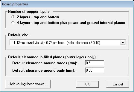
The final printed design will have nice clear traces and big fat chunky pads which are easier to solder onto. Even if you're using a household iron to transfer the toner from the press-n-peel onto the copper board, the relatively thick traces and spacing between them should allow you to get away with a little movement during ironing (always a problem, and can cause smudged and broken traces when thinner lines are used).
When you transfer the image onto the copper board, it will, naturally be reversed. For example, pin1 on all your microchips is suddenly on the top-right hand corner, not the top-left. Don't panic - this isn't a mistake! That's exactly what you want, because the PCB image is on the bottom of your board. If you turn it over and place the components on the top (non-copper) side of the board, you should find that all the pads line up with the components perfectly (pin1 on the top side of the board is on the top-left, but turn the board over and it magically appears on the top-right side of a set of pins - because you're looking at the bottom of the chip, not the top).
Why use ExpressPCB?
It's free.
It's easy.
You can create drill files from it!
Creating drill files from ExpressPCB
Here's a simple VB app that will parse an xaml file generated from an ExpressPCB PDF and plot the points for drilling in a separate file, and a g-code.
That's sound like more than it is, so let's look at what's involved:
Firstly, create your schematic and PCB layout in ExpressPCB. When placing pads, use pads with 2.03mm size and 0.89mm hole:

Print the top copper layer to a PDF file using CutePDF

Open the PDF file in Inkscape and save as .xaml
The .xaml file should open with later versions of Internet Explorer (amongst others) so you can check the conversion worked properly. Open the file in Notepad to see all the complex XML shape descriptions.

Now start up the VB app and provide it with the path to the .xaml file

There are a few parameters to mess about with here. The main one is the code that describes a circle. If you've used 2.03mm pads with 0.89mm holes, this should be c -7 0 -12 -5 -12 -11 0 -7 5 -12 12 -12 6 0 11 5 11 12 0 6 -5 11 -11 11. You should see this set of commands repeated throughout the .xaml file, each time preceeded by [mX Y] type commands. If you've used different pad sizes, look for something similar - a repeating set of draw commands at different positions, with a fill colour of #FFFFFFFF (the [mX Y] commands are movement commands, the fill colour is white: basically we're looking for the repeating white circles that make up the centre of all the pads).
At the minute, we're not sure what units the .xaml file uses compared to our CNC machine - it will take a bit of messing about to get this right, so there's a scale multiplier parameter. As the app finds all the drill holes, it applies this multiplier, to convert from screen units/co-ordinates to whatever units the CNC machine uses. The final parameters to set at the Z-axis movement axis. The app will create some G-Code which can be loaded straight into the CNC controller software (we use Mach3 but may change once the demo version runs out!). Depending on whether the machine is set up to use inches, mm, or some other unit, this value may need to be changed - it defines the start (retracted) and end (plunged) position of the Dremel for drilling.
Pressing the "create files" button generates two files - one an amended .xaml file, so you can see a preview of the drill pattern generated. Load this into Internet Explorer (or some other software that lets you view .xaml) so see the final output.
 The original and amended .xaml files showing drill hole positioning
The VB app also creates a CNC-ready G-Code file with the points plotted, complete with "move-to" commands and "extend/retract drill head" commands.

Load the G-Code into the CNC controlling software and let it go!
Download the VB app here
That's sound like more than it is, so let's look at what's involved:
Firstly, create your schematic and PCB layout in ExpressPCB. When placing pads, use pads with 2.03mm size and 0.89mm hole:

Print the top copper layer to a PDF file using CutePDF

Open the PDF file in Inkscape and save as .xaml
The .xaml file should open with later versions of Internet Explorer (amongst others) so you can check the conversion worked properly. Open the file in Notepad to see all the complex XML shape descriptions.

Now start up the VB app and provide it with the path to the .xaml file

There are a few parameters to mess about with here. The main one is the code that describes a circle. If you've used 2.03mm pads with 0.89mm holes, this should be c -7 0 -12 -5 -12 -11 0 -7 5 -12 12 -12 6 0 11 5 11 12 0 6 -5 11 -11 11. You should see this set of commands repeated throughout the .xaml file, each time preceeded by [mX Y] type commands. If you've used different pad sizes, look for something similar - a repeating set of draw commands at different positions, with a fill colour of #FFFFFFFF (the [mX Y] commands are movement commands, the fill colour is white: basically we're looking for the repeating white circles that make up the centre of all the pads).
At the minute, we're not sure what units the .xaml file uses compared to our CNC machine - it will take a bit of messing about to get this right, so there's a scale multiplier parameter. As the app finds all the drill holes, it applies this multiplier, to convert from screen units/co-ordinates to whatever units the CNC machine uses. The final parameters to set at the Z-axis movement axis. The app will create some G-Code which can be loaded straight into the CNC controller software (we use Mach3 but may change once the demo version runs out!). Depending on whether the machine is set up to use inches, mm, or some other unit, this value may need to be changed - it defines the start (retracted) and end (plunged) position of the Dremel for drilling.
Pressing the "create files" button generates two files - one an amended .xaml file, so you can see a preview of the drill pattern generated. Load this into Internet Explorer (or some other software that lets you view .xaml) so see the final output.
 The original and amended .xaml files showing drill hole positioning
The VB app also creates a CNC-ready G-Code file with the points plotted, complete with "move-to" commands and "extend/retract drill head" commands.

Load the G-Code into the CNC controlling software and let it go!
Download the VB app here
Saturday, June 18, 2011
SimpleBotis Community Forum
Hello and welcome to the all new forum for SimpleBotics. At this forum you can meet other robotic hobbyists and talk about robotics! You can also join now!
SimpleBotics Community
SimpleBotics Community
Friday, June 17, 2011
Robo-Roundup #18
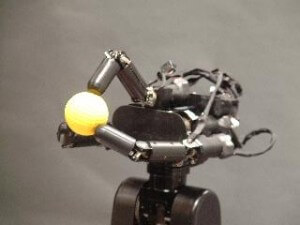
1. These swarm robots are like no other: http://spectrum.ieee.org/automaton/robotics/artificial-intelligence/kilobots-are-cheap-enough-to-swarm-in-the-thousands
2. Robot and senator have a argument: http://spectrum.ieee.org/automaton/robotics/robotics-software/us-senator-calls-robot-projects-wasteful
3. Check out this very cool dino-bot: http://www.plasticpals.com/?p=28143
4. Kindergartners and museum visitors love this robot: http://www.plasticpals.com/?p=28181
Well, that sums up this week's roundup, so thanks for reading and be sure to comment below!
Subscribe to:
Posts (Atom)